Ceramic PCBs for High-Altitude Applications
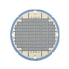
Ceramic PCBs
Ceramic PCB boards can withstand high temperatures, and can also operate in corrosive and vibratory circuit conditions. Moreover, they are highly resistant to erosion due to their tough material construction. This makes them the ideal choice for heavy-duty applications, such as medical devices and aerospace electronics. However, there are some drawbacks to using ceramic PCBs. First, they are more expensive than standard FR-4 boards. Also, they can be fragile and break if handled improperly.
To mitigate these drawbacks, many manufacturers use laser rapid activation metallization (LAM) technology to create ceramic boards. This method allows the ceramic material to be quickly bonded to metal, so that it is not exposed to the elements that cause oxidation. This prevents the corrosion that would otherwise affect the performance of the board.
Another benefit of using ceramic pcb board is their ability to handle high currents for long periods of time. This is especially important for electronic devices that are required to work at high altitudes. Ceramic PCBs also have low electrical resistance and a low coefficient of thermal expansion, which is ideal for high-frequency circuits.
Ceramic PCBs for High-Altitude Applications
The most popular ceramic PCB materials are alumina and aluminum nitride. The former has a thermal conductivity of 24W/mK and a CTE of about 10W/mK. It can be found in a wide range of consumer products and industrial equipment, including LED ship lights and trucks. The latter has a thermal conductivity of 7 to 10 times that of alumina, and can be made with varying thicknesses. It can be used in LED solar battery modules and high-power integrated circuits.
Depending on the application, there are various types of ceramic PCBs. For example, some are designed for high temperatures, and are known as High-Temperature Co-fired Ceramic (HTCC) circuits. To make these circuits, raw ceramic materials are mixed with adhesive, lubricant, solvent, and plasticizer to form the ceramic base layer. Then, it is coated and baked at 1600 to 1700 degrees Celsius for up to 48 hours after lamination. This baking process is done in a gaseous environment, such as hydrogen gas.
After printing and stacking the ceramic layers, the fabricator will fire the entire stack in an oven. The firing temperature is usually below 1000°C, which matches the sintering temperature of the metal traces. This is an advantage of using ceramic over FR-4, as it eliminates the need for OSP or HASL finishes.
The main drawback of ceramic PCBs is their cost, which is a result of the special materials and manufacturing processes that are used to make them. However, the increased reliability and performance of these circuits makes them a worthwhile investment for a variety of applications. They are ideal for applications that require a high degree of precision and a rugged design. In addition, they are ideal for industries that require a high frequency of data and signal transmissions, such as the medical and aerospace industries. They can also withstand high pressure and temperature, which is not possible with traditional PCBs.