The Role of Pick-and-Place Machines in Flex Rigid PCB Manufacturer
Pick-and-Place Machines in Flex Rigid PCB Manufacturer
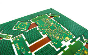
Rigid flex PCBs offer many benefits, including reduced package size and weight, increased mechanical flexibility and durability, and improved electrical performance. They are used in applications such as mobile communications devices, wearables, and foldable electronics. Rigid flex circuit boards are made from a combination of rigid and flexible sections, and the design must be carefully considered to ensure both structural reliability and electrical functionality.
Rigid-flex PCBs require specialized fabrication techniques, making them more expensive than rigid FR4 boards. However, careful consideration of the different options available and a strong working relationship with the rigid-flex fabricator throughout the design phase can yield significant cost savings.
The first step in the flex rigid pcb manufacturer is to pre-etch the two layers of the flex circuit using a standard etching technique, either by dipping them into an etch bath or spraying an etch solution onto the surface of each layer. Then, the circuit pattern on each side of the flex circuit is mechanically drilled through both layers with precision drilling systems or technologies.
Next, the circuit holes are filled with copper and chemically plated through. These plated through holes are important for connecting the conductive layers of the flex circuit to the rigid board sections. The holes also need to be sized correctly for the intended application. Oversized holes can cause stress and breakage, while undersized ones will cause short circuits during assembly. Depending on the application, blind or buried vias can be used to minimize space constraints in the inner layers.
The Role of Pick-and-Place Machines in Flex Rigid PCB Manufacturer
After the copper plating, the circuit is finished with an additional layer of protective coverlay that acts as a solder mask and a thermal barrier between the metal layers of the flex and the rigid materials. The coverlay material is typically an additional polyimide film with adhesive, though adhesive-less processes are available. A photo-imageable solder mask can be applied as well to selected areas of the flex circuit, allowing for precise placement of components.
The etched rigid and flex circuits are then bonded together with a pressure-sensitive adhesive or heat-resistant epoxy to form the final panel. This bonding process is critical for ensuring the rigid-flex PCB will stay flat during final assembly and reflow in a reflow oven. The resulting bonded panel is then cut to size and trimmed for a clean finish.
Stiffeners can be added to selected areas of the flex circuit, adding strength and stiffness to specific regions to help it resist mechanical damage during assembly and operation. The addition of these stiffeners increases the total thickness of the flex circuit and can increase manufacturing costs slightly.
Rigid-flex PCBs can reduce packaging size and weight and improve device performance, especially in high-density applications. In addition, they can replace wire harnesses in some applications, saving time and cost during assembly. They also make it easier to perform automated testing and inspection. This allows manufacturers to build circuitry that fits the device instead of forcing the device to fit the circuitry.