The Purpose of an Assembled Circuit Board
Purpose of an Assembled Circuit Board
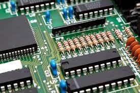
A circuit board is a complex structure that contains the essential components and electrical connections to make an electronic device work. It is also known as a printed circuit board assembly (PCBA). An assembled circuit board is the finished product that can then be connected to other circuit boards or plugged into an external component to function. It is important to know the assembly process as it plays a crucial role in the creation of functional electronic devices.
The first step in the PCB assembly process is constructing the circuit board itself. This involves creating a substrate to which a layer of conducting copper will be added. The substrate acts as a mechanical support for the circuit and an insulator between the different layers. The conductive copper layer is added by applying a thin coating of copper foil to both sides of the substrate using a lamination process. The foil is then bonded to the substrate by heating and pressure. The result is a single-sided or double-sided printed circuit board.
Next, the circuit board is designed in a CAD software program. The schematic diagram is a symbolic representation of the circuit that will be built on the board, showing each component and its connection to other components. Once the design is complete, it must be converted into a layout, which shows the board’s exact size and shape and its component locations. The layout must also contain the conductive pathways, which are called nets in a CAD program. It is the designer’s job to route these nets for optimal performance while being mindful of areas of excessive heat and noise and physical obstructions such as connectors, cables, and mounting hardware.
The Purpose of an Assembled Circuit Board
Once the layout is finalized, it will be converted into manufacturing files, called Gerber files. These files will be sent to a circuit board manufacturer, who will use them to create the actual circuit board. Single-sided and double-sided boards both have a layer of copper on one side that’s used for incorporating different electronic components. Multi-layer circuit boards have additional internal layers that allow for more intricate wiring patterns.
Once a board has been created, it can be drilled to accept the component leads. For through-hole technology, the component leads are inserted into holes that’re surrounded by conductive pads or lands on the surface of the board. The pins on the component are lined up with these pads and held in place by solder paste, which has been applied to them. For surface-mount technology, the components are placed on top of the bare circuit board.
The final steps in the assembly process involve placing the component leads, soldering and inspection. This includes visual inspection, automated optical inspection, and JEDEC guidelines for component placement, soldering, and reflow. Once the solder has cooled, it holds the component firmly in place. A circuit board can then undergo a series of functional tests to ensure that it does what it was designed to do.